
Wireless Power
Wireless power transfer eliminates the need for a power connector during charging, enabling more compact device designs while improving water and dust resistance and enhancing usability by removing the need to attach and detach charging cables.
ROHM’s 13.56 MHz wireless charging IC integrates the power control firmware within the IC itself despite its compact package, eliminating the need for an external host MCU. When combined with a compact antenna optimized for the 13.56 MHz high-frequency band, it enables the implementation of a wireless power system even in space-constrained designs. The IC is suitable for wearable devices such as smart rings and stylus pens, as well as rotating applications including e-bike torque sensors, enhancing both design flexibility and system reliability. In addition, it supports contactless communication and power transfer using Near Field Communication (NFC) technology, enabling system designs that integrate authentication, data communication, and power delivery.
Videos & Catalogs


Parametric Search

Supporting Information
Product Features
Feature 1A super small chip with the power receiver function, build-in software removes the need for software development
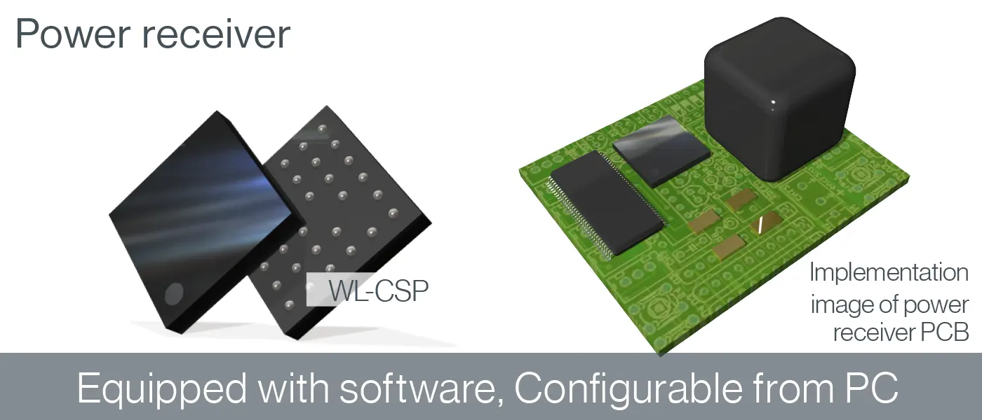
The power receiving LSI incorporates the power receiving function into a small WL-CSP package or a highly reliable QFN package.
In addition, both the power receiving LSI and power transmission LSI are equipped with software, eliminating the need for program development.
Individual user settings can be configured using a PC tool provided by ROHM.
Feature 2Equipped with NFC Forum Type3 Tag function
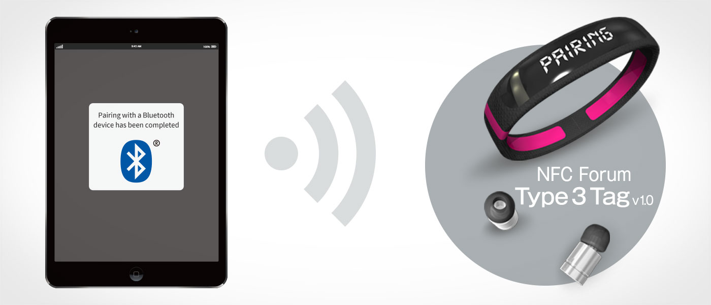
The power receiving LSI is equipped with NFC Forum Type3 Tag function.
This function is a ROM function that can read fixed data written in advance in the built-in 496Byte Data Flash in NDEF format* . It is also possible to communicate with an external NFC reader/writer through Tag data.
NDEF format: NFC Data Exchange Format A data format used for data exchange in NFC.
Feature 3Driven at 5V can mobilize the entire system
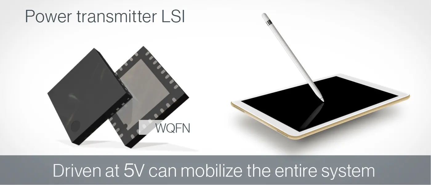
The power transmission LSI has a power supply voltage of 5 V and can be driven by a single power supply.
Since the power receiving LSI does not require a power supply, it can be configured as a power transmission LSI + power receiving LSI + device to be charged, enabling the entire system to be mobile.
Feature 4Optimization of the power transmitter
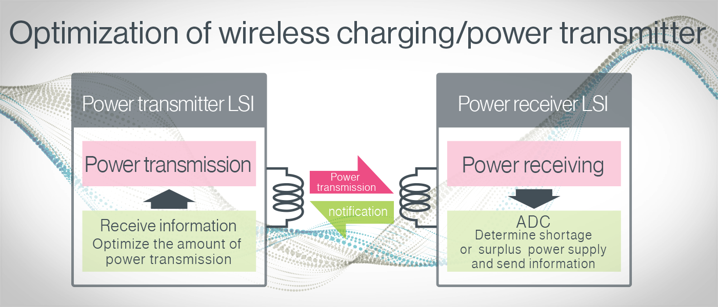
The power transmission LSI has the function of adjusting the power transmission.
On the other hand, the power receiving LSI uses the built-in ADC to determine the excess or shortage of power supply based on the voltage after rectification and the unnecessary current flowing through the built-in shunt regulator.
And notifies the information to the power transmission LSI, which can eliminate unnecessary power transmission and optimize the power transmission.
Feature 5High-level safety by the detection function of foreign objects and the dropout of the device
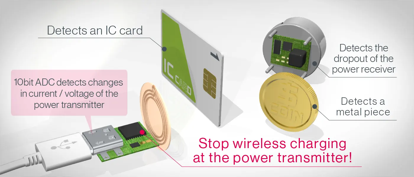
The power transmission LSI uses a built-in 10-bit ADC to detect changes in the power transmission current, detect it as a foreign object, and stop wireless charging. It detects metal pieces and IC cards to prevent heat generation and destruction.
It also detects when the receiving LSI is out of the feeding range to prevent unwanted power transmission.
Applications

ROHM’s 13.56 MHz wireless power charging ICs are ideally suited for building wireless charging systems for compact devices such as stylus pens and hearable devices equipped with secondary batteries of around 200 mAh. In addition to battery charging, some ICs can be applied to devices that require both wireless power transfer and data communication.


"LAPIS TECHNOLOGY™" is a trademark or a registered trademark of ROHM Co., Ltd.